Step 2: Layer stack and spectra |
  
|
Step 2: Layer stack and spectra |
|
The layer stack that we have to define is very simple: Assuming that the backside of the silicon substrate is rough and that there is no significant contribution from the backside we have just one anisotropic layer of molecules on a 'silicon halfspace'.
Open the list of layer stacks and from there the standard stack that is already there. Drag the silicon optical constants to the bottom halfspace. Then create between the two halfspace objects a new layer of type 'Anisotropic layer'. Click with the right mouse button the column labeled 'See parameters'. The following dialog opens:

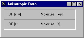
Surely you can guess already how to continue: Starting in the treeview, drag the materials that describe the molecular response to the locations labeled 'none'. The dialog should now look like this:
That's all for the layer stack definition. Now open the list of spectra to do the settings that define the simulated infrared spectra.
Change the name of the default spectrum to '20'. Open its window to set the angle of incidence to 20 degrees. Switch from s- to p-polarization.
Then create three additional spectra and name them '40', '60' and '80'. Use these values as angles of incidence. Select p-polarization in all cases.
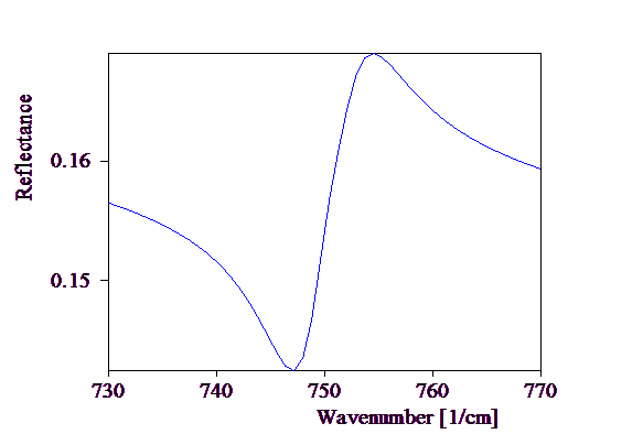
Now use the Range command in the main window of SCOUT to set the spectral range of all dielectric function models and all spectra to 730 ... 770 1/cm with 50 spectral points. Open all spectra by right-clicking their corresponding treeview items and press the 'a' key to autoscale the graphs. You should get the following spectra:
20°:

40°:
60°:

80°:

In case you had problems to follow the instructions above you can load the configuration tu2_ex2_step2.sc2 which contains the model developed up to now.