R vs. total thickness during deposition |
  
|
R vs. total thickness during deposition |
|
Optical monitoring charts displaying the reflectance of a layer stack vs. total layer stack thickness are computed by objects of type 'Optical growth monitor' that are created in the list of distributions. These objects are handled almost exactly like Electric field distributions.
The difference is, of course, that the reflectance instead of the electric field is computed. In addition, the meaning of the x-axis differs. Here x represents the total thickness of the layer stack. If x is negative, SCOUT computes the reflectance of the blank substrate. Starting at x=0 SCOUT computes how the reflectance of the layer stack changes while the layers are growing. Like in the deposition, SCOUT starts a new layer if the present one has reached its final thickness.
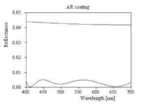
As an example, an anti-reflection coating with 4 layers (note that this is just a demo to demonstrate the optical monitoring and not a professional filter design) and the following structure is used:
Type Material Thickness
1 Halfspace Vacuum
2 Thin film SiO2 87.6 nm
3 Thin film ZrO2 121.2 nm
4 Thin film SiO2 35.1 nm
5 Thin film TiO2 4.7 nm
6 Halfspace Glass Type BK7
The optical constants are all taken from the SCOUT database.
The reflectance spectra of the blank substrate (red curve) and the final coating are shown in the next graph:
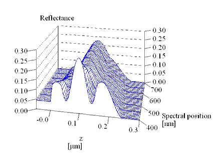
The optical growth monitor shows the development from the blank substrate to the final reflectance. You can choose a 2D picture

or 3D representations:
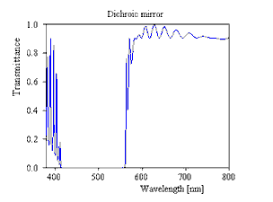
A more advanced example is a dichroic mirror (design published in [Park 1997]) of this structure:
1 Halfspace Vacuum
2 Thin film ZrO2 29.2 nm
3 _Begin superlattice Repeat 27 times
4 Thin film SiO2 88.9 nm
5 Thin film ZrO2 58.5 nm
6 _End superlattice
7 Thin film SiO2 88.9 nm
8 Thin film ZrO2 29.2 nm
9 Halfspace Glass Type BK7
The final transmittance spectrum at 45 deg angle of incidence and s-polarisation is this:
Optical monitoring data for reflectance at normal incidence of light are shown in the next graph:
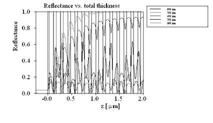
Based on data like this, the monitoring strategy is to be developed in order to find the right moment to stop the growth of a layer and to start with the next material. In addition to knowledge of the reflectance vs. total thickness, one may be interested also in the time dependent reflectance signal which is computed by a similar SCOUT object discussed below.