EL example |
  
|
EL example |
|
Here is a simple EL example. The emitting layer is a porous silicon layer on a silicon wafer, covered with a thin gold film.
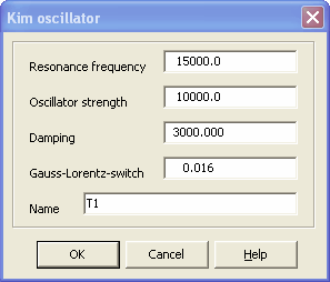
The internal emission spectrum is modeled by a single Kim oscillator with the following parameters:
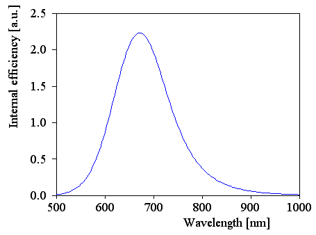
This leads to the following spectrum:
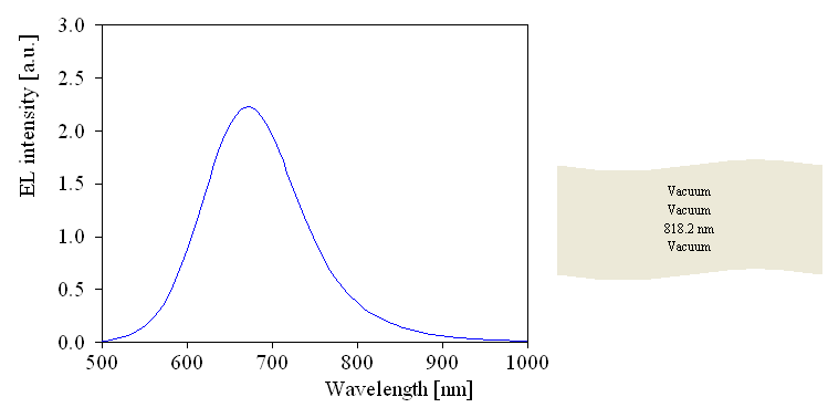
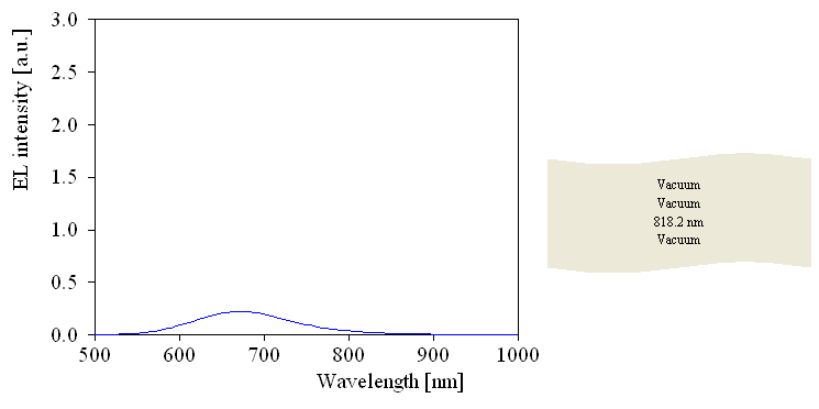
In order to make clear how the EL computation in SCOUT works, we will build up the stack step by step. Let's start with a single light-emitting thin film in between two halfspaces. All materials are vacuum - this is not really realistic, of course, but we can see the pure emission without any reflectance effects at the interfaces between the layers.
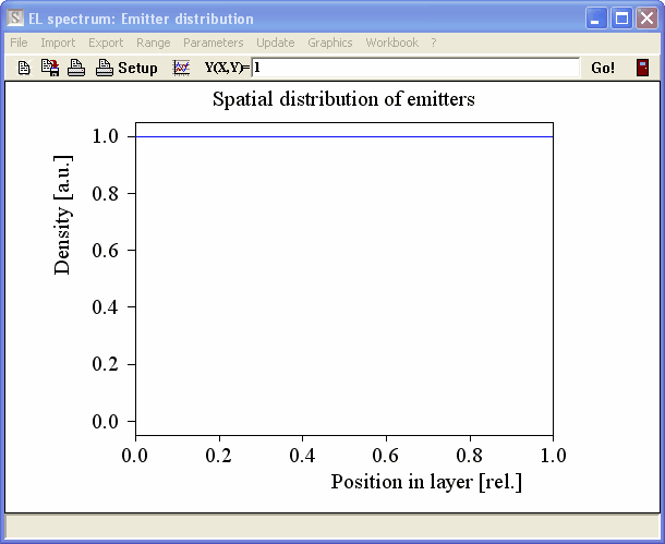
The depth distribution of the light emission within the EL active layer is sampled with 50 points - i.e. there are 50 light sources in the emitting layer, placed at equidistant positions. The light sources can have a depth-dependent strength of emission which is taken from a user-defined depth distribution. Click on the Distribution button to see this function. Let's start with the simple assumption that the light emission is distributed equally within the active layer, i.e. all points contribute with weight 1:
The EL spectrum computation now takes all the 50 points, sums up the output for each one and divides by the number of points.In the present case the outcome on the reflectance side of the sample is the original internal emission spectrum:
We assume now that the EL emission is not homogeneously distributed within the layer stack but has the following depth profile:
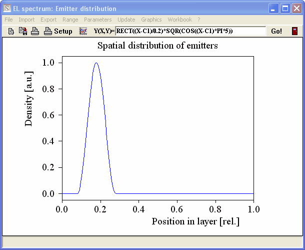
The parameter C1 in the formula allows to move the peak from the top to the bottom of the layer. You can do that, for example, with a slider (horizontal or vertical bar object) in a view. The parameters C1 to C6 of the user-defined distribution formula will appear as possible fit parameters in SCOUT.
The emitted spectrum is now the following:
The average emission probability of the 50 points is now much less than 1 - hence the emission is much lower now.
Note that the EL emission into a certain observation direction is computed adding up two contributions: One is the internal emission that aims directly into the wanted external direction (taking into account the change of direction due to refraction at the interfaces). The second one is the emission into the direction which is reflected into the wanted direction by the backside of the emitting layer. This second contribution should contribute to the spectrum if we place a silicon wafer below the emitting layer. The next graph compares the previous spectrum (vacuum backside,red curve) with the one obtained with a silicon wafer substrate (blue):
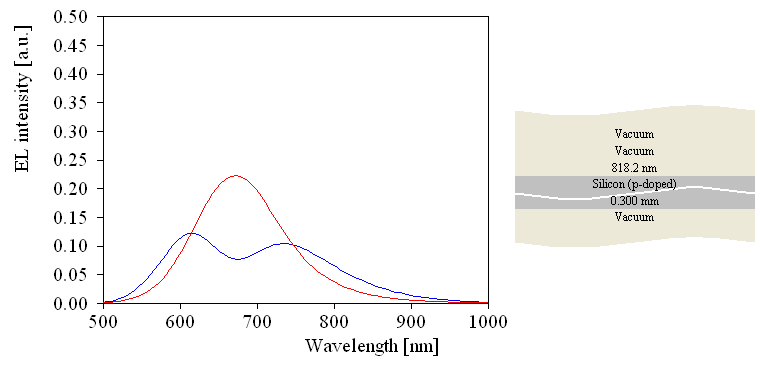
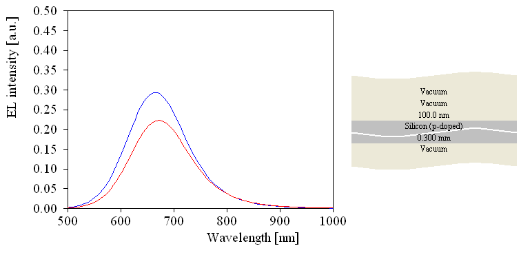
Well, in some spectral regions the backside reflected contribution leads really to an increase in EL emission, but in the main peak there is less light observed with silicon substrate. Assuming that the light emission is coherent in all directions, SCOUT superimposese the two contributions discussed above fully coherent. This leads to interference patterns in the spectra which strongly depend on the thickness of the EL emitting layer. Here is the result for a thinner emitting layer:
We can now replace the material 'Vacuum' of the active layer by porous silicon. The emission spectrum changes to the following:
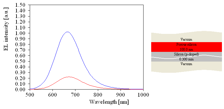
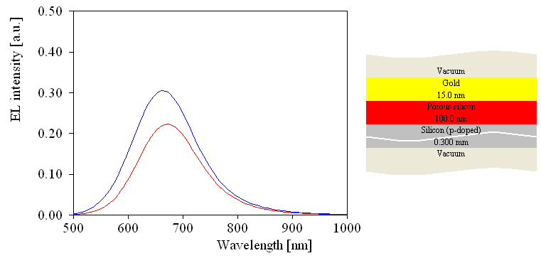
Finally we add the gold layer on top which reduces the emission significantly:
Placing some sliders in the main view gives you some freedom to manually change parameters:
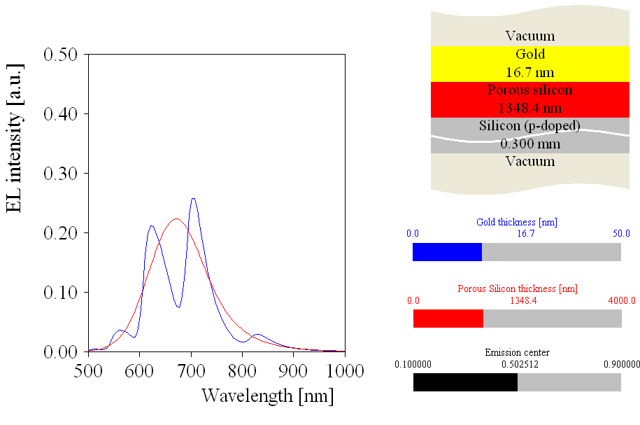
Note that interference effects strongly modify the shape of the EL spectrum. The observed peaks cannot be directly interpreted as internal emission channels.